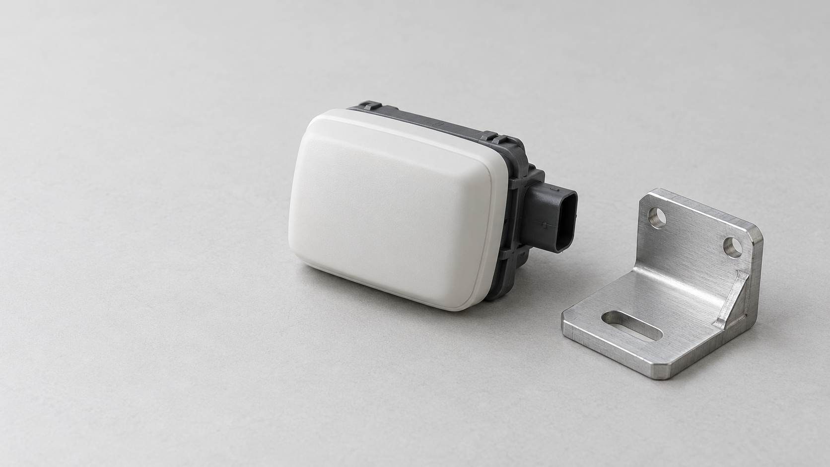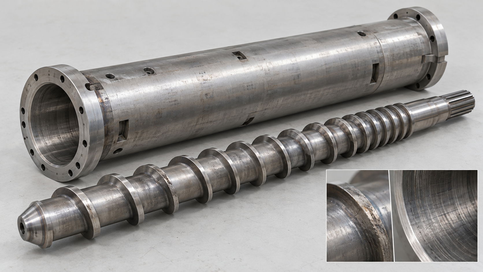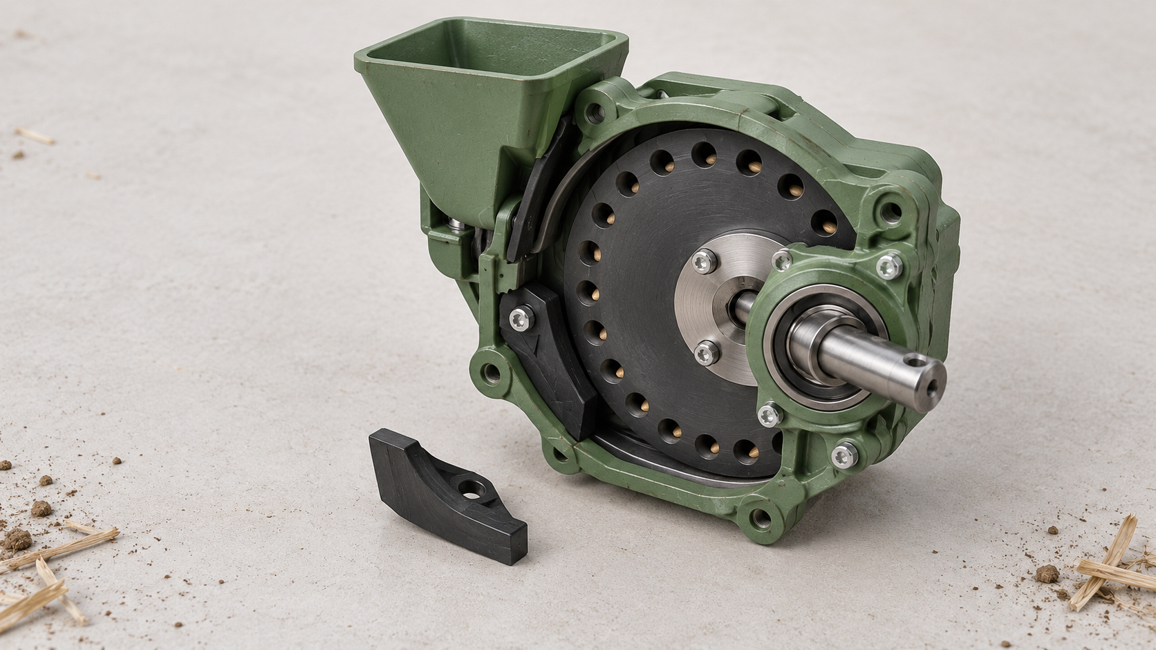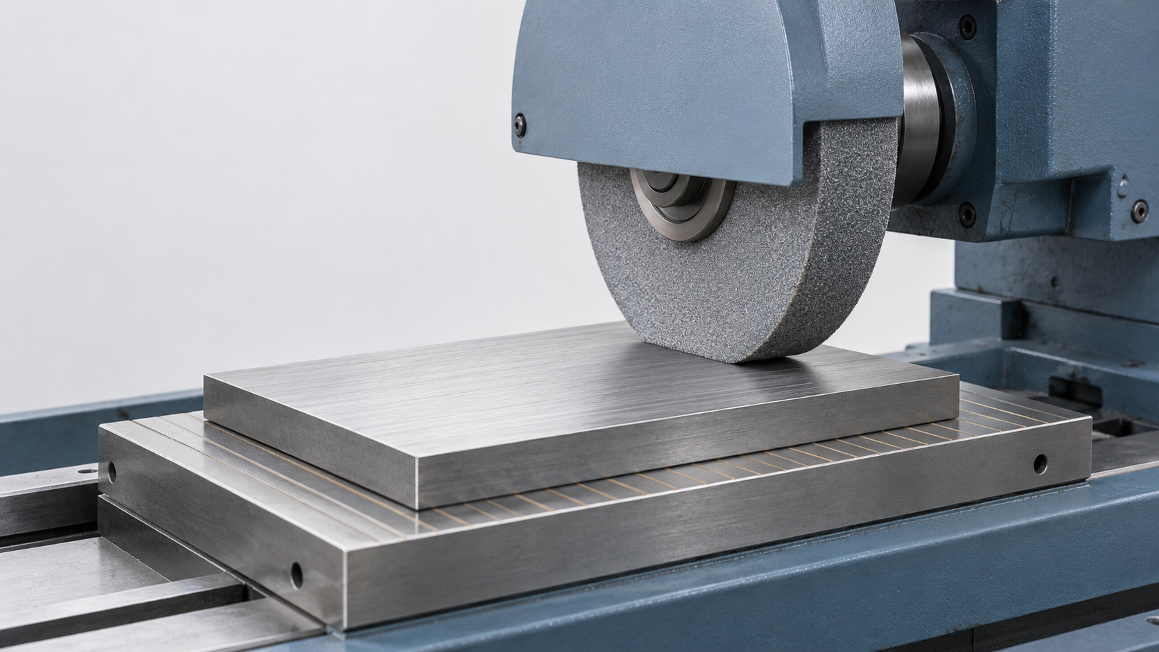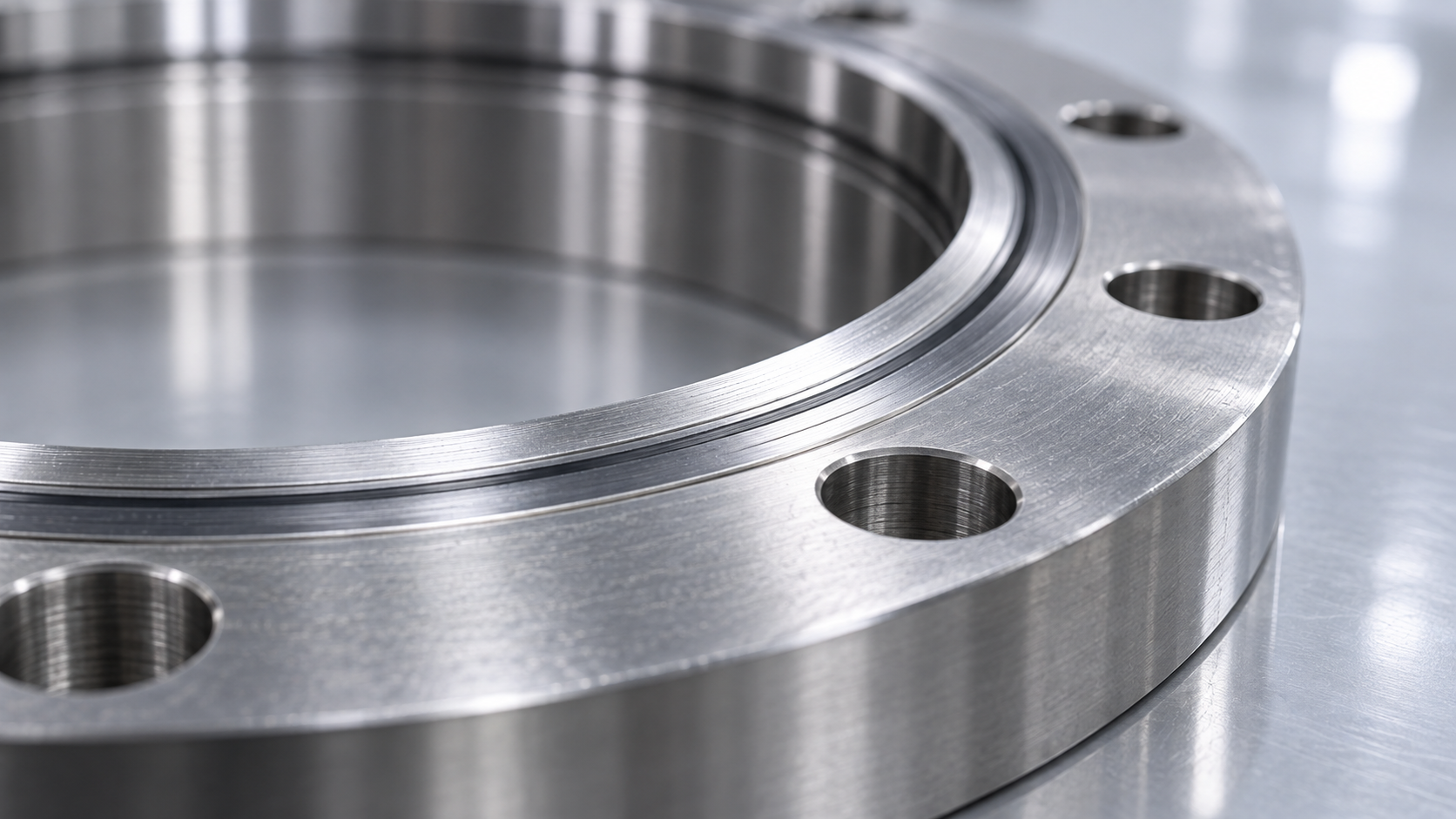
Why Semiconductor Parts Are Difficult: First Determine Which Category They Belong To
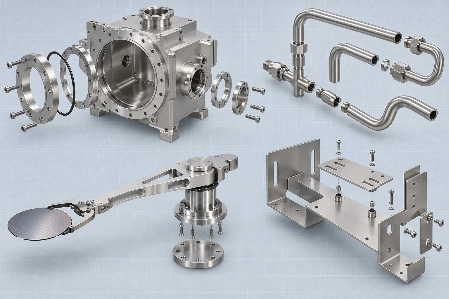
Put the word "semiconductor" on a purchase order, and what it points to can vary enormously. What lands on machining, sheet metal, vacuum casting, and injection molding workstations is usually not the wafer itself, but a ring of hardware surrounding the wafer: front-end equipment chambers, gas line components, vacuum flanges and sealing faces, wafer transfer and clamping components, cleanroom peripheral structures and fixtures, as well as metal parts around packaging molds and lead frames. This article discusses the manufacturability of these parts—how to draw the drawing, how to select materials, how to allocate tolerances, and how to inspect—not chip design or wafer processes themselves.
Separate the categories first, and the difficulties become clear. The core of chamber and flange parts is the sealing face and vacuum integrity; a single scratch can scrap the part. Transfer and clamping components must be light, rigid, and thermally stable, with thin walls and cantilever structures being the norm. Tubing components are limited by internal bore machinability; deep cavities and cross holes are difficult to polish properly. Cleanroom peripheral structures and fixtures are often treated as ordinary sheet metal parts, but particle shedding and cleaning residue can cause problems just the same. The same drawing may say "semiconductor," yet the process route can be completely different.
It is advisable to fix the order of judgment: first confirm the part's function (vacuum, corrosion resistance, thermal conduction, or insulation), then determine the material, and only then the process and tolerances. Reverse the order, and you will end up forcing an unnecessary precision with a difficult-to-machine material, or conversely, applying ordinary tolerances to a sealing face. The following sections unfold in this order.
Material Feasibility: When Selecting Materials for Semiconductor Parts, First Check Whether They Can Be Machined
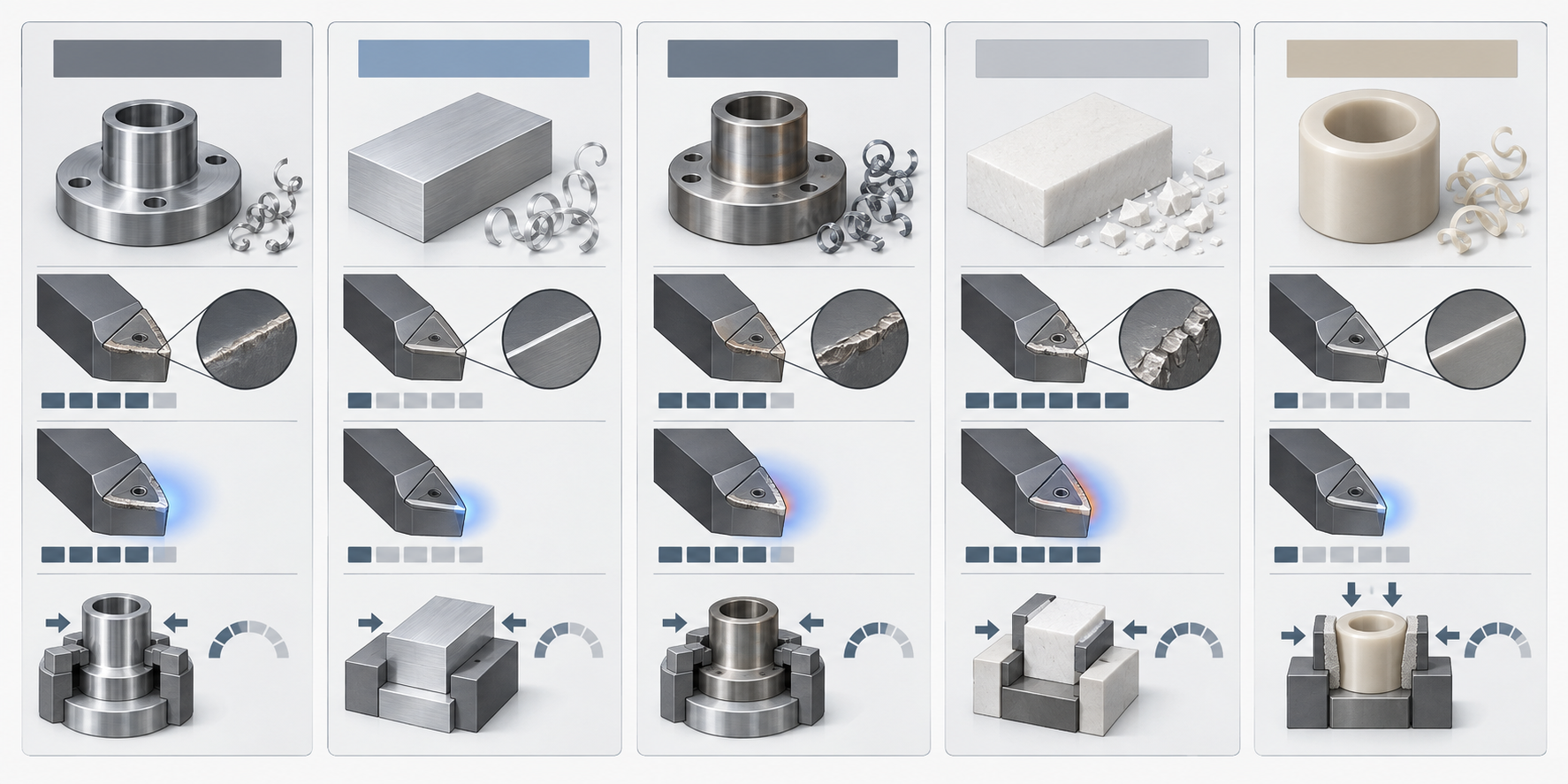
Many people start material selection for semiconductor equipment parts with "which material has the best performance," which easily goes wrong at the DFM stage. A smoother approach is the reverse: first look at the functional boundaries, then the material, then the process, and finally the tolerance numbers. If a drawing changes 6061 to 17-4PH, it may be more corrosion-resistant functionally, but on the machining side it immediately adds tool wear, cutting heat, and subsequent stress relief issues—the tolerance band hasn't changed, but the cost has shifted up a notch.
Materials that land on machining and forming orders for semiconductor peripherals roughly fall into several categories. Among stainless steels, 304 and 316L are used for chambers and gas line components, with 316L more common in clean and corrosion-resistant scenarios; 17-4PH is often used for structural parts requiring both strength and corrosion resistance, but dimensions change before and after solution aging. Aluminum alloy 6061 is easy to machine and has good thermal conductivity; 7075 is stronger but more likely to cause thin-walled parts to deflect during cutting. Kovar and molybdenum are used for sealing components that need thermal expansion matching with glass or ceramics, and belong to the difficult-to-machine category. Ceramic parts such as alumina and aluminum nitride rely on diamond grinding and are not suitable for marking according to metal tolerance conventions. Among engineering plastics, PEEK, PTFE, PPS, and PI each have their own emphases; PTFE is soft and difficult to clamp, while PEEK is sensitive to cutting temperature.
How Materials Amplify Tolerance Pressure
The problem with difficult-to-machine materials is not the phrase "can't be cut," but that they amplify errors from fixturing and thermal deformation. Materials like Kovar and molybdenum have poor thermal conductivity, so cutting heat concentrates near the cutting edge, and thin-walled parts change dimensions after cooling. The age hardening of 17-4PH is accompanied by shrinkage; if aging is done after rough machining, sufficient finishing allowance must be left. PTFE has a large coefficient of linear expansion, so a room-temperature difference during measurement can consume half a tolerance band. In other words, if the material is chosen wrong, all subsequent tolerance allocation must change accordingly.
Order of Judgment: Function → Material → Process → Tolerance
Running through the parameters in this order can save a lot of back-and-forth.
- Function: Which of vacuum, corrosion resistance, thermal conduction, or insulation does this part serve? A vacuum sealing face must not have through porosity; corrosion-resistant parts must not use grades prone to pitting; thermally conductive parts must consider interface thermal resistance.
- Material: On the premise of satisfying function, prioritize good machinability. If 6061 works, don't use 7075; if 304 works, there's no need for 17-4PH, unless there are hard requirements for strength or thermal expansion matching.
- Process: Once the material is set, the process route is basically constrained. Ceramics go to grinding, Kovar goes to low-speed heavy-depth-of-cut or electrical machining, plastics go to sharp-edge high-rake tools.
- Tolerance: Only at the end are tolerances allocated to each face. Marking ±0.01 before the previous step is settled is mostly making trouble for the supplier.
A common industry practice is to first mark functional and non-functional faces separately, relaxing non-functional faces by one grade. If material selection for semiconductor parts is done solidly, the subsequent process and tolerances have room for negotiation; conversely, locking down tolerances first and then selecting materials is usually the most expensive path. The feasibility of specific grades still needs to be confirmed according to the drawing and the supplier's tooling and fixturing conditions.
From Drawing to Machining: Fixturing, Deformation, and Tolerance Allocation for Semiconductor Parts
Once semiconductor parts go to CNC machining, the difficulty is not making the dimensions, but the clamping force deforming the part during fixturing. Thin-walled chambers, long cantilevers, sealing faces, deep-cavity internal bores—these feature types recur in vacuum chambers, gas line components, and wafer transfer parts, and their tolerance loss is often determined not by whether the tool is good enough, but by the positions of clamping points and support points. If fixturing is not considered at the drawing stage, after quoting it can only be compensated by multiple setups and fitting, doubling the cost.
Where Fixturing Deformation Comes From: Clamping Logic for Thin-Walled Chambers and Long Cantilevers
When a thin-walled chamber (such as a vacuum chamber with 2–3 mm wall thickness) is clamped on the outer diameter with a three-jaw chuck, it springs back after release, and roundness is lost. A common industry practice is to switch to soft jaws, expanding sleeves, or vacuum chucks, distributing clamping force over surfaces rather than points; long cantilever parts need auxiliary supports or a tailstock to hold them, otherwise cutting force causes chatter. The criterion is simple: if the part measures qualified in the free state but out of tolerance when clamped, the problem is fixturing. Writing "measure in free state" clearly on the drawing is more effective than tightening tolerances.
Datum Consistency and Multiple Setups: When It's Worth Flipping the Part One More Time
Semiconductor parts often require two or even three setups, because sealing faces and deep-cavity internal bores are often not accessible from the same direction. The principle is datum consistency: in the first operation, first machine the locating face that all subsequent operations will use, and all later flips reference it. If a deep-cavity internal bore requires too much tool overhang, vibration degrades both the bore wall Ra and cylindricity; in that case, it is better to flip the part one more time and bore from both ends than to force a long tool through in one pass. The criterion: when tool overhang exceeds 4 times the holder diameter, first consider changing the process route rather than the cutting parameters.
Cost-Driven Tolerances: Which Faces Must Be Tight, and Which Can Be Relaxed
The most common problem on semiconductor part drawings is that all dimensions are marked with the same tolerance grade. Sealing faces (O-ring grooves, metal sealing lips) and mating faces indeed need to be tight, because leakage or failure to assemble is a functional failure; but non-sealing contour faces, non-mating mounting hole positions, and cable routing grooves have no functional impact when relaxed by one grade, while machining saves a finishing pass or an inspection. Grouping functional and non-functional faces on the drawing compresses cost more than tightening everything overall. The specific grade depends on your vacuum level target and gauge capability; it is recommended to mark a list of functional faces on the drawing and let the supplier derive tolerances from function, rather than copying the markings.
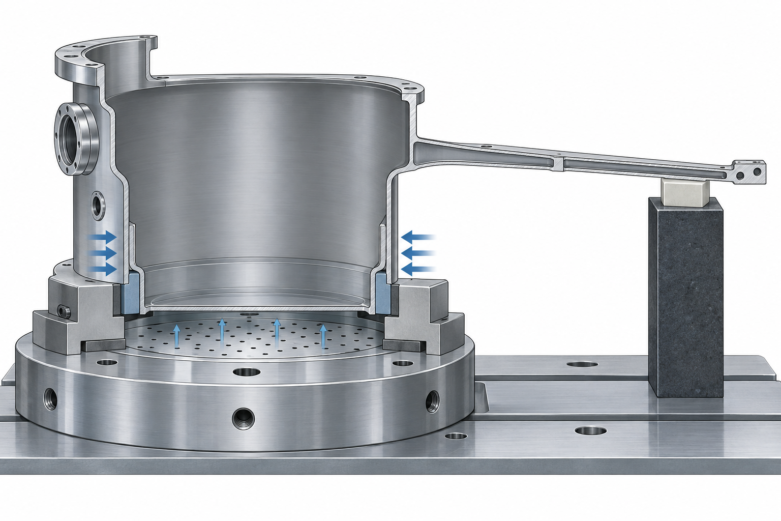
If a part has both thin walls and a sealing surface, prioritize ensuring the datum and clamping stability of the sealing surface; the thin-wall area can be temporarily reinforced with process bosses and then cut off after machining—this approach must be aligned with the supplier in advance, otherwise they may simply say "it can't be done."
Surface, cleanliness, and post-processing: semiconductor requirements easily missed on drawings
The easiest thing to miss on semiconductor part drawings is not dimensional tolerances, but surface and cleanliness requirements. Dimensions are specified, but roughness is not; roughness is specified, but particles and outgassing are not; by the time assembly or machine installation reveals seal surface leakage, particles shedding from the chamber, or plastic parts outgassing, the cost of rework far exceeds the machining itself. This section discusses surface, cleanliness, and post-processing together because they constrain each other: the choice of post-processing directly determines how much allowance to leave in prior machining and which tools to use.
Roughness and sealing surfaces: lower Ra is not always better
Vacuum flanges, O-ring sealing surfaces, and gas line interfaces commonly use Ra 0.8 or below; when higher requirements apply, Ra 0.4 or even 0.2. But there is a common misconception here: a sealing surface is not better the smoother it is. A mirror finish (Ra below 0.05) is actually unfavorable for certain elastomer seals, because the surface is too smooth for the seal ring to achieve microscopic interlocking, making it prone to slipping under micro-motion. A common industry practice is to control metal sealing surfaces at Ra 0.4–0.8 with appropriate flatness; rubber seals can be relaxed to Ra 1.6. Specific values must be confirmed according to the sealing type and cannot be copied blindly.
Roughness also constrains the machining method in turn. Ra 0.8 is generally achievable by fine milling or fine turning; Ra 0.4 requires grinding or polishing after fine turning; Ra 0.2 or below often requires electropolishing or hand lapping. Writing Ra 0.2 on a drawing is equivalent to telling the supplier an additional process step is needed, and both quotation and lead time will change. Therefore, roughness should be specified on functional surfaces only; do not casually specify it on all non-functional surfaces.
Particles, outgassing, and cleaning: how to write cleanliness requirements into drawings
Semiconductor equipment is sensitive to particles and organic outgassing. Residual cutting fluid, polishing paste, and glove prints from machining are inconsequential on ordinary parts, but on chambers or wafer transfer components they are contamination sources. Drawings should specify: cleaning method (ultrasonic cleaning, deionized water rinsing, solvent cleaning), cleanliness level (e.g., by particle size and count), and whether silicon-containing or halogen-containing lubricants are permitted. Plastic parts (PEEK, PTFE, PI) also require attention to outgassing rates, and vacuum baking for degassing should be required when necessary.
- Sealing surface scratches: damaged during clamping or transport; Ra meets spec but local scratches cause seal failure. Require deburring, edge blunting, and protection between process steps.
- Cleaning residue: insufficient rinsing after ultrasonic cleaning leaves residual cleaning agent that outgasses under vacuum. Rinsing water quality and drying method must be specified.
- Coating peeling: nickel plating or passivation for corrosion resistance, with poor adhesion due to inadequate pre-treatment, peeling under vacuum or thermal cycling.
Post-processing must be scheduled into the process route in advance
Post-processing such as passivation, electropolishing, and plating cannot be an afterthought once machining is complete. They change dimensions: electropolishing typically removes a few microns to tens of microns, and plating increases thickness. If critical dimensions have tolerances, post-processing allowance must be reserved in advance. In addition, the sequence of post-processing also affects results—whether to chamfer first then polish, or polish first then chamfer, produces different edge quality. Writing post-processing into the process route prevents omissions at the quotation stage.
Inspection plan determines the process route: a tolerance that cannot be measured is no tolerance at all
Critical dimensions of semiconductor parts are often hidden in internal cavities, sealing surfaces, or deep holes, and these are precisely the hardest locations to measure. CMM styli can reach into deep cavities, but are limited by stylus ball diameter and shaft rigidity; vision measurement is fast but can only see contours and surface features; 3D scanning can cover complex curved surfaces but still has blind spots for deep grooves, blind holes, and internal steps. A tolerance that cannot be measured can only be estimated by experience on the machining side, and ultimately verified through assembly—this is one of the main sources of rework for semiconductor parts.
Therefore, the inspection plan must be determined before quotation, not after the part is made when searching for gauges. How to select datums, what gauges to use, which dimensions must be fully inspected, and which can be sampled—these decisions in turn constrain the clamping method and machining sequence. For example, for a seal groove in a vacuum chamber, if the gauge is a flat plate plus plug gauge, then the datum surface during machining must be unified with the gauge datum surface; otherwise the measured values are meaningless. First define datums, then define gauges, then define the process—this order cannot be reversed.
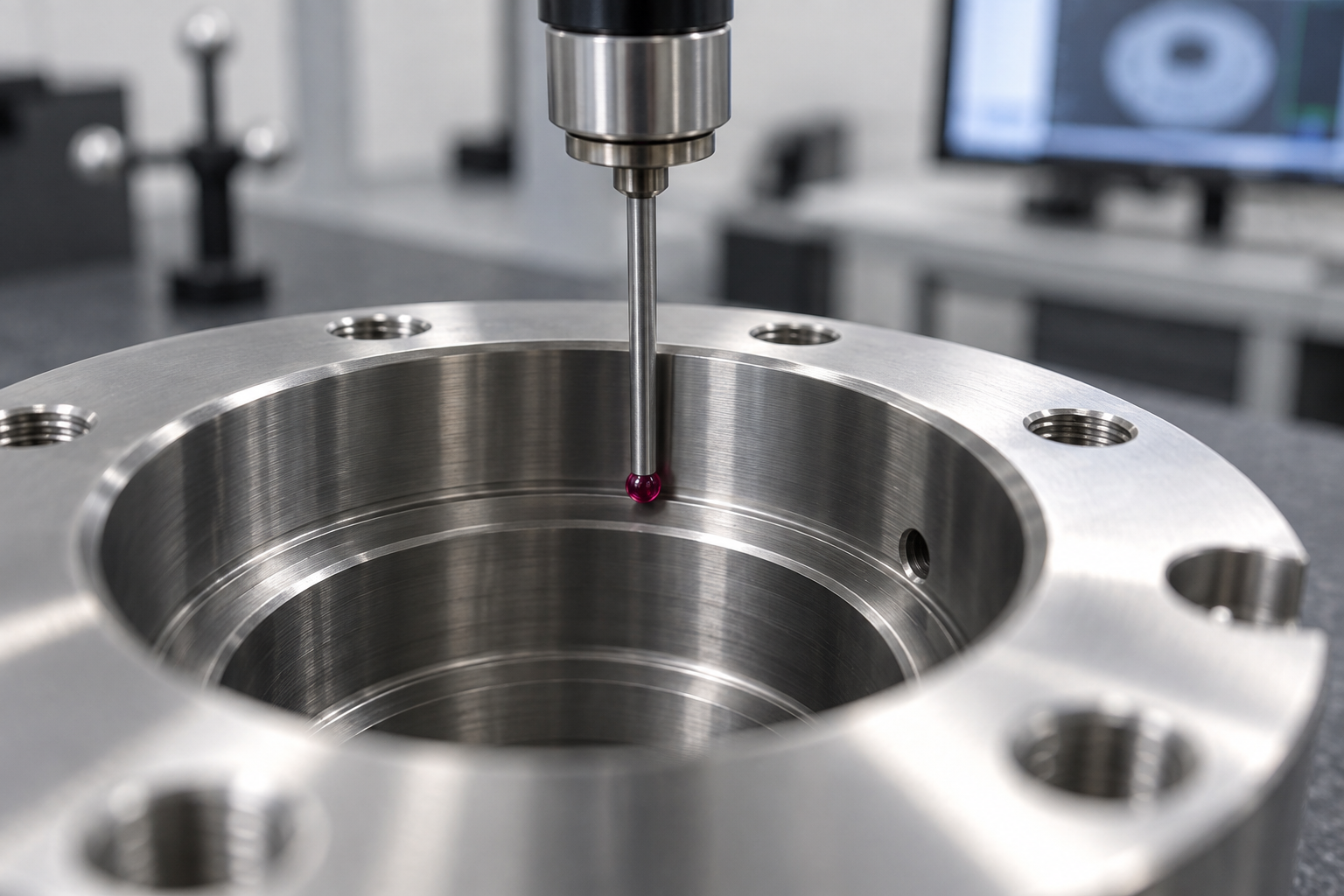
Align datums and gauges first, then the clamping sequence can be determined
A common mistake in actual production is: the drawing specifies position tolerance but no datum; or a datum is specified, but the gauge is aligned to a different surface. In semiconductor parts, the relative relationship between sealing surfaces, mounting surfaces, and internal cavity axes is often more important than individual dimensions. If the inspection datum and machining datum are inconsistent, an additional alignment clamping step is needed during machining, increasing both cost and deformation risk. An actionable criterion is: first confirm whether the datum can be stably reproduced by the gauge, then decide whether a dedicated gauge is needed, and only then arrange the machining sequence. If the gauge itself lacks precision, even the best machine tool cannot measure the true error.
For small-batch trial production, 3D scanning can quickly provide an overall deviation color map, suitable for first-article comparison and reverse confirmation, but it cannot replace quantitative measurement of critical dimensions. A common industry practice is to use scanning for global screening and CMM for critical dimension determination; which to use specifically must be confirmed according to drawing tolerances and inspection costs. The earlier the inspection plan is determined, the fewer detours the process route will take.
Selecting processes by part type: the boundaries of CNC, sheet metal, vacuum casting, and injection molding
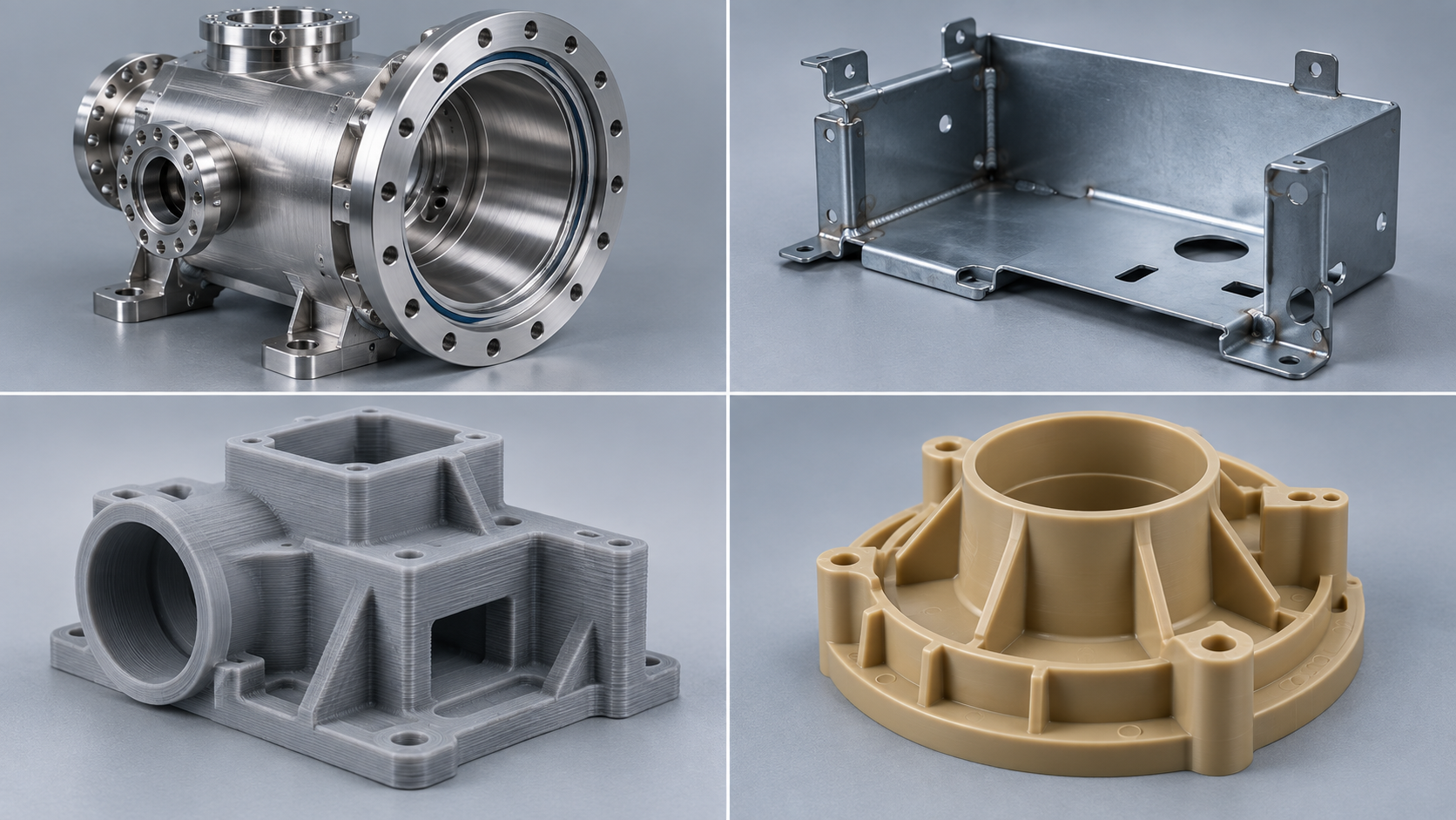
For parts on semiconductor equipment that fall into machining orders, process boundaries determine success or failure more than "precision." First look at part function: pressure-bearing, gas-conducting, insulating, structural support, or merely masking. Different functions allow different processes. Below is a decision line for the four common part categories.
Chambers and flange parts: CNC is the default starting point
Vacuum chambers, gas distribution blocks, and flange sealing surfaces are typically dominated by CNC milling. Features such as the bottom surface roughness of seal grooves, flatness of flange faces, and straightness of deep cavity bores are more stable when machined in a single setup on a turn-mill or five-axis machine than with multiple setups. If the chamber is large, thin walls and long cantilevers introduce deformation, requiring soft jaws or vacuum chucks for assistance. A common industry practice is to relax non-sealing surface tolerances by one grade and shift the saved labor hours to sealing surface lapping, which is more cost-effective overall. Whether this applies still depends on the usage conditions and cleanliness requirements specified on the drawing.
Cleanroom enclosures and brackets: sheet metal tube structures cannot handle sealing
Stainless steel enclosures, equipment brackets, and cable tray covers around cleanrooms are more economical with sheet metal bending and welding. The boundaries of sheet metal are: bend radii, post-weld deformation, and flatness typically cannot meet sealing surface requirements, and particle shedding is difficult to control. If an enclosure also provides vacuum sealing, the entire part should not be made of sheet metal; instead, the sealing flange should be split into a CNC part and assembled with the sheet metal housing. With this split, machining and welding each do their own part, and inspection is easier to define.
Small-batch trial production: distinguishing the uses of 3D printing and vacuum casting
The trial production stage often requires a few to a few dozen pieces. 3D printing is suitable for verifying shape, assembly relationships, and flow channel routing, but most printed parts are inferior to metal in vacuum, high temperature, and outgassing performance. Vacuum casting (handboard replication) can produce plastic parts with an appearance close to injection molding, suitable for structural verification and early assembly demonstrations, but likewise does not guarantee sealing and cleanliness. The common boundary for both is: use them only to verify "it fits and it looks right," and do not use them to replace sealing and cleanliness testing of functional parts.
Batch plastic parts: injection molding depends on tooling and draft
Once engineering plastic parts such as PEEK and PPS enter batch production, the cost structure of injection molding becomes viable. Additional requirements for injection molded parts in semiconductor scenarios are low outgassing and dimensional stability: uneven wall thickness causes sink marks and warping, seal groove locations must have sufficient draft, and gate locations affect weld line strength. These must be determined before tooling is cut; modifying tooling is far more expensive than modifying drawings.
To turn a drawing into an evaluable quotation, the key is not to ask for unit price first, but to first clearly describe the part type, material, critical surfaces, and inspection plan. For quick verification, you can use AI chat quotation, submitting the drawing and functional description together, so the supplier can provide feedback based on process boundaries rather than quoting a vague "high precision."
Revise the drawing before quoting: a DFM checklist for semiconductor parts
First separate functional and non-functional surfaces, then discuss tolerances
Unify datums and write the inspection plan into the requirements
- Mark functional surfaces and non-functional surfaces, and assign tolerance grades separately; do not let the entire drawing have a single requirement.
- Unify datums and draw datum symbols on surfaces that can be fixtured and measured.
- Relax tolerances on non-critical features; cost is often reduced at this step, not in machining.
- Write surface and cleanliness requirements clearly: Ra, particles, outgassing, cleaning method; if any item is missing, a process step will need to be added later.
- Clarify the inspection plan: which dimensions to measure, what equipment to use, and who issues the report.
- Mark deburring and chamfering requirements; burrs near sealing surfaces will directly cause leakage.
Frequently Asked Questions (FAQ)
The following are several questions readers most often ask after reading the previous sections. The answers all center on the manufacturability boundaries of semiconductor parts and do not involve specific lead times or prices.
Do all semiconductor parts require very high precision?
No. Precision is concentrated only on functional surfaces such as sealing surfaces, mating surfaces, and datum surfaces; relaxing non-functional surfaces by one grade usually does not affect use and can significantly reduce machining difficulty. Marking functional and non-functional surfaces separately on the drawing is more effective than tightening everything overall.
Can difficult-to-machine materials be replaced with alternative materials?
It depends on the functional constraints. Kovar, molybdenum, and ceramics are often used for thermal expansion matching, thermal conduction, or insulation, and replacing them with stainless steel or aluminum may destroy these characteristics. If it is only a structural support part, there is greater room for substitution, but thermal expansion and corrosion resistance requirements must be rechecked.
How should surface and cleanliness requirements be written into the drawing?
Write the upper limit of Ra, whether scratches are allowed, particle and outgassing limits, and the cleaning and passivation methods. Writing only "clean" is not executable. These requirements will change the process route, so it is best to mark them before quotation to avoid later rework.
Who defines the inspection plan?
Usually the designer and the machinist confirm it together before quotation. If critical dimensions are in internal cavities or deep holes, a CMM may not be able to measure them, so inspection tools or a scanning plan need to be agreed in advance. A tolerance that cannot be measured is equivalent to no tolerance.
Which process should be chosen for small-batch trial production?
For cavities and flanges, prioritize CNC; for housings and brackets, sheet metal can be used; when the shape is complex and the quantity is very small, use 3D printing or silicone molding; only consider injection molding once plastic parts are confirmed for mass production. The basis for selection is the part type and quantity, not the superiority or inferiority of a single process.
Key takeaways
- The difficulty of semiconductor parts usually lies not in single-point precision, but in the mutual constraints among materials, fixturing, inspection, and cleanliness.
- Assess material feasibility before discussing tolerances: difficult-to-machine materials amplify fixturing and thermal deformation errors, so tolerances must follow the process.
- Cost-driven tolerances are the core lever: relaxing a non-functional surface by one grade often reduces cost more than changing equipment.
- The inspection plan must be defined before quoting: a tolerance that cannot be measured is no tolerance at all—gauges and datums often determine the process route.
- Surface and cleanliness requirements (particles, outgassing, roughness) must be written into the drawing, otherwise rework is likely at the post-processing stage.